Memory Basics: RAM, ROM, and Flash
Introduction
Imagine a computer without memory—it would be like having a brilliant mind but no ability to remember anything. Every time you turn it off, everything disappears. Every program would need to be rebuilt from scratch. That's why memory is just as crucial as processing power.
Digital memory stores information—programs, data, images, everything. Understanding how memory works is essential for:
- Embedded systems design
- Microcontroller programming
- Computer architecture
- Digital system design
- IoT devices
In this lesson, we'll explore the fundamental types of digital memory and how they work at the circuit level.
Your smartphone has several types of memory working together: DRAM for running apps, Flash for storage, ROM for boot code, SRAM for cache. Each type serves a specific purpose based on its characteristics!
Memory Fundamentals
What is Memory?
Memory is a digital storage device that can:
- Store binary information (write operation)
- Retrieve that information later (read operation)
- Maintain information over time (retention)
Memory Classification
Digital Memory
├── Volatile (loses data when power off)
│   ├── SRAM (Static RAM)
│   └── DRAM (Dynamic RAM)
└── Non-Volatile (retains data when power off)
    ├── ROM (Read-Only Memory)
    ├── PROM (Programmable ROM)
    ├── EPROM (Erasable PROM)
    ├── EEPROM (Electrically Erasable PROM)
    └── Flash Memory
Key Memory Parameters
| Parameter | Description |
|---|---|
| Capacity | Total storage (bits, bytes, KB, MB, GB) |
| Organization | Width × Depth (e.g., 1K × 8 = 8K-bit memory) |
| Access Time | Time to read/write data |
| Volatile/Non-volatile | Loses/retains data without power |
| Read/Write | Can data be modified? |
| Cost per Bit | Price per stored bit |
| Power Consumption | Energy required to operate |
| Density | Storage per unit area |
Memory Capacity and Organization
Notation:
- K = 1,024 (2^10)
- M = 1,048,576 (2^20)
- G = 1,073,741,824 (2^30)
Organization Format: Width × Depth
- Width: Number of bits per location (data bus width)
- Depth: Number of locations (address space)
Examples:
| Organization | Total Bits | Address Lines | Data Lines |
|---|---|---|---|
| 1K × 1 | 1,024 bits | 10 (2^10 = 1K) | 1 |
| 1K × 8 | 8K bits (1 KB) | 10 | 8 |
| 64K × 8 | 512K bits (64 KB) | 16 | 8 |
| 1M × 8 | 8M bits (1 MB) | 20 | 8 |
Address Calculation:
Example: 64K locations needs 16 address lines (2^16 = 64K)
Memory Architecture
Basic Memory Block

Key Signals:
1. Address Bus (A0-An)
- Selects which memory location to access
- Unidirectional (input only)
- Width determines capacity: n bits = 2^n locations
2. Data Bus (D0-Dm)
- Carries data to/from memory
- Bidirectional (can be input or output)
- Width determines word size (typically 8, 16, 32 bits)
3. Control Signals
- CS̄ (Chip Select): Activates the chip (active LOW)
- WĒ (Write Enable): Controls read/write (LOW = write, HIGH = read)
- OĒ (Output Enable): Enables output drivers (active LOW)
Memory Operations
Read Operation:
1. Place address on address bus
2. Set CS̄ = 0 (select chip)
3. Set WĒ = 1 (read mode)
4. Set OĒ = 0 (enable output)
5. Data appears on data bus after access time
Write Operation:
1. Place address on address bus
2. Place data on data bus
3. Set CS̄ = 0 (select chip)
4. Set WĒ = 0 (write mode)
5. Data stored in selected location

SRAM (Static RAM)
How SRAM Works
SRAM stores each bit in a bistable flip-flop circuit (typically 6 transistors).
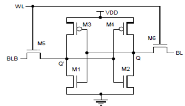
Structure:
- 6T Cell: Most common (6 transistors per bit)
- Two cross-coupled inverters form bistable latch
- Two access transistors connect to bit lines
- Word line enables access
SRAM Characteristics
| Feature | Value/Description |
|---|---|
| Speed | Very fast (1-10 ns) |
| Volatility | Volatile (loses data when power off) |
| Density | Low (6 transistors per bit) |
| Power | Low static, higher than DRAM |
| Refresh | Not needed |
| Complexity | Simple interface |
| Cost | Expensive per bit |
Read Operation:
- Word line activated (selects row)
- Bit lines sense stored value
- Sense amplifiers detect small voltage difference
- Data output
Write Operation:
- Word line activated
- Bit lines driven to desired value
- Access transistors conduct
- Flip-flop forced to new state
SRAM Applications
1. CPU Cache
- L1, L2, L3 cache in processors
- Needs to be extremely fast
- Cost less critical due to small size
2. Microcontroller RAM
- Working memory for embedded systems
- Fast access crucial for performance
3. FPGA Block RAM
- On-chip memory in FPGAs
- Fast local storage
4. Networking Equipment
- Routers, switches need fast buffers
- SRAM provides speed for packet processing
Commercial SRAM ICs:
| IC | Organization | Speed | Notes |
|---|---|---|---|
| 6264 | 8K × 8 | ~45 ns | Classic, widely used |
| 62256 | 32K × 8 | ~55 ns | Common in embedded systems |
| CY7C199 | 32K × 8 | ~15 ns | Fast SRAM |
| AS7C4096 | 512K × 8 | ~10 ns | High capacity |
SRAM is used where speed is critical and capacity is limited. Your CPU's cache is SRAM because even a few nanoseconds matter at GHz clock speeds!
DRAM (Dynamic RAM)
How DRAM Works
DRAM stores each bit as charge on a capacitor (1 transistor + 1 capacitor).
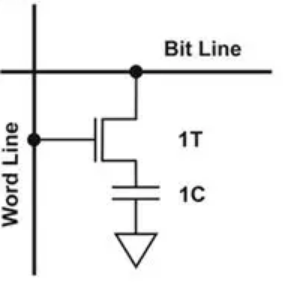
Structure:
- 1T1C Cell: 1 transistor + 1 capacitor per bit
- Much denser than SRAM (4-6× more storage per area)
- Capacitor holds charge representing 0 or 1
DRAM Challenges
1. Charge Leakage
- Capacitor slowly loses charge
- Data gradually fades (milliseconds)
- Solution: Periodic refresh
2. Destructive Read
- Reading discharges capacitor
- Solution: Sense amplifiers recharge after read
3. Refresh Requirement
- Each cell must be refreshed every ~64ms
- Refresh cycles "steal" bandwidth from normal access
- Typically auto-refreshed by controller

DRAM Characteristics
| Feature | Value/Description |
|---|---|
| Speed | Slower than SRAM (30-80 ns) |
| Volatility | Volatile (loses data when power off) |
| Density | Very high (1 transistor per bit) |
| Power | Low per bit, but refresh adds power |
| Refresh | Required every 64ms |
| Complexity | Complex controller needed |
| Cost | Cheap per bit |
DRAM Types Evolution
Asynchronous DRAM (Traditional)
- Simple interface, slower
- Access time ~60-80 ns
Synchronous DRAM (SDRAM)
- Clocked operation, synchronized
- Burst mode access
- Access time ~10-15 ns
DDR SDRAM (Double Data Rate)
- Transfers data on both clock edges
- DDR, DDR2, DDR3, DDR4, DDR5
- Each generation faster and more power efficient
Comparison:
| Type | Year | Clock | Transfer Rate | Voltage |
|---|---|---|---|---|
| SDR SDRAM | 1996 | 100-166 MHz | 100-166 MT/s | 3.3V |
| DDR | 2000 | 100-200 MHz | 200-400 MT/s | 2.5V |
| DDR2 | 2003 | 200-533 MHz | 400-1066 MT/s | 1.8V |
| DDR3 | 2007 | 400-1066 MHz | 800-2133 MT/s | 1.5V |
| DDR4 | 2014 | 800-2133 MHz | 1600-4266 MT/s | 1.2V |
| DDR5 | 2020 | 1600-3200 MHz | 3200-6400 MT/s | 1.1V |
DRAM Applications
1. System RAM (Main Memory)
- Computers, servers, workstations
- Large capacity needed (GB to TB)
- Cost-effective for bulk storage
2. Graphics Memory (VRAM)
- GPU memory for frame buffers
- High bandwidth versions (GDDR)
3. Smartphones/Tablets
- LPDDR (Low-Power DDR)
- Optimized for battery life
4. Embedded Systems
- Systems needing large RAM (>1MB)
- Cost-sensitive applications
SRAM is fast but expensive and less dense. DRAM is slower but cheap and dense. Modern systems use SRAM for cache (speed) and DRAM for main memory (capacity). Best of both worlds!
ROM (Read-Only Memory)
What is ROM?
ROM is non-volatile memory with data permanently stored during manufacturing. It cannot be modified (hence "read-only").
ROM Characteristics
| Feature | Value/Description |
|---|---|
| Speed | Fast (20-50 ns) |
| Volatility | Non-volatile (permanent) |
| Programmability | Programmed at factory |
| Modification | Cannot be changed |
| Cost | Economical for mass production |
| Reliability | Very high (no write cycles to fail) |
ROM Applications
1. Firmware Storage
- BIOS/UEFI in computers
- Bootloader code
- System initialization
2. Lookup Tables
- Mathematical functions (sin, cos, log)
- Character generators (fonts)
- Conversion tables
3. Control Logic
- Fixed sequences in controllers
- State machine implementation
4. Embedded Systems
- Code that never changes
- Safety-critical systems
Despite the name, modern systems rarely use true ROM. Instead, they use Flash memory which can be updated but is still non-volatile. We'll cover Flash next!
PROM, EPROM, EEPROM
PROM (Programmable ROM)
PROM is ROM that can be programmed once by the user.
Structure:
- Fusible links at each bit location
- Programming "blows" fuses to create pattern
- One-time programmable (OTP)
Programming:
Virgin PROM: All 1s (fuses intact)
Programming: Blow fuses to create 0s
Result: Permanent pattern
Use Case:
- Small-volume production
- Prototyping
- Security (cannot be read back easily)
EPROM (Erasable PROM)
EPROM can be erased with UV light and reprogrammed.
Key Feature: UV Erasure
- Quartz window in IC package
- UV light (253.7 nm) for 15-20 minutes
- Erases entire chip (cannot erase selectively)
- Cover window with label to prevent accidental erasure
Characteristics:
- Non-volatile storage
- Reprogrammable (but slow erasure)
- 10-20 year data retention
- ~10,000 erase cycles
Common EPROM:
- 27C256: 32K × 8 EPROM
- 27C512: 64K × 8 EPROM
EEPROM (Electrically Erasable PROM)
EEPROM can be erased and programmed electrically, byte by byte.
Advantages Over EPROM:
- ✅ No UV light needed
- ✅ In-circuit programming
- ✅ Selective erasure (byte-level)
- ✅ Faster erase (~5-10 ms per byte)
EEPROM Cell:
- Similar to EPROM (floating gate)
- Additional tunnel oxide for electrical erasure
- Quantum tunneling removes charge
Characteristics:
- ~1,000,000 erase cycles (much more than EPROM)
- Slower than SRAM/ROM for reading
- More expensive than Flash
- Ideal for small amounts of changeable data
Applications:
- Configuration data in embedded systems
- User preferences, settings
- Calibration data
- Serial numbers, MAC addresses
- Odometer data in cars
Common EEPROM ICs:
| IC | Organization | Interface | Notes |
|---|---|---|---|
| 24C02 | 256 bytes | I2C | Very common |
| 24C64 | 8K bytes | I2C | Larger capacity |
| 24C256 | 32K bytes | I2C | High capacity |
| 25LC640 | 8K bytes | SPI | Fast serial |
The 24Cxx series EEPROMs are incredibly popular in embedded systems. With just 2 wires (I2C), you can add non-volatile storage for settings, calibration, logs, etc.
Flash Memory
The Modern Standard
Flash memory combines the best features of EPROM and EEPROM. It's the dominant non-volatile storage today.
Key Advantages:
- ✅ Electrically erasable (like EEPROM)
- ✅ Block erasure (faster than byte-by-byte)
- ✅ High density (like DRAM)
- ✅ Non-volatile (like ROM)
- ✅ Inexpensive (mass production)
Flash Types
NOR Flash:
- Random access (like SRAM)
- Fast read (10-50 ns)
- Slow write/erase
- Execute-in-place (XIP) capable
- Used for code storage
NAND Flash:
- Sequential access (like hard drive)
- Slower read (25-50 µs per page)
- Fast write/erase
- Very high density
- Used for bulk storage
Comparison:
| Feature | NOR Flash | NAND Flash |
|---|---|---|
| Read Speed | Fast | Moderate |
| Write Speed | Slow | Fast |
| Cost per Bit | Higher | Lower |
| Density | Lower | Higher |
| Interface | Parallel | Serial/Parallel |
| Random Access | Yes | No (page-based) |
| XIP | Yes | No |
Flash Memory Structure
Flash Cell:
- Floating gate transistor
- Charge trapped = logical state
- No leakage (non-volatile)
Organization:
- Pages: Smallest write unit (256B - 4KB)
- Blocks: Smallest erase unit (4KB - 128KB)
- Must erase before writing (erase sets all bits to 1)
Flash Characteristics
| Feature | Value/Description |
|---|---|
| Speed (read) | Fast (NOR) / Moderate (NAND) |
| Speed (write) | Slow (need erase) |
| Volatility | Non-volatile |
| Erase Cycles | 10,000-100,000 (SLC) / 1,000-10,000 (MLC) |
| Retention | 10+ years |
| Wear Leveling | Required for longevity |
| Cost | Very economical |
Flash Memory Types by Cell
SLC (Single-Level Cell)
- 1 bit per cell
- Faster, more reliable
- 100,000 erase cycles
- More expensive
- Used in industrial/enterprise
MLC (Multi-Level Cell)
- 2 bits per cell
- Slower, less reliable than SLC
- 10,000 erase cycles
- Cheaper
- Consumer SSDs
TLC (Triple-Level Cell)
- 3 bits per cell
- Even cheaper
- 3,000-5,000 cycles
- Consumer products
QLC (Quad-Level Cell)
- 4 bits per cell
- Cheapest per bit
- 1,000 cycles
- High-capacity storage
Flash has limited write cycles. For applications with frequent writes (data logging), implement wear leveling or use technologies like FRAM that have unlimited endurance.
Flash Applications
1. Microcontroller Program Storage
STM32, ESP32, Arduino bootloader
Stores code that runs on power-up
2. USB Flash Drives
Portable storage
NAND Flash with USB controller
3. SD Cards / Memory Cards
Cameras, phones, embedded systems
NAND Flash with SD/MMC interface
4. Solid State Drives (SSDs)
Replacing hard drives in computers
NAND Flash with SATA/NVMe interface
Multiple chips in parallel for speed
5. Embedded Systems
Configuration, data logging, file systems
NOR for code, NAND for data
6. IoT Devices
Firmware storage and updates
Over-the-air (OTA) update capability
Memory Comparison Summary
| Type | Volatile | Speed | Density | Cost/bit | Typical Size | Use Case |
|---|---|---|---|---|---|---|
| SRAM | Yes | Very Fast | Low | High | KB-MB | Cache, fast buffers |
| DRAM | Yes | Fast | High | Medium | MB-GB | Main memory |
| ROM | No | Fast | Medium | Low | KB-MB | Firmware (legacy) |
| EPROM | No | Fast | Medium | Medium | KB | Legacy systems |
| EEPROM | No | Moderate | Low | High | Bytes-KB | Settings, config |
| NOR Flash | No | Fast read | Medium | Medium | MB | Code storage |
| NAND Flash | No | Moderate | Very High | Low | GB-TB | Bulk storage |
Memory Hierarchy in Modern Systems
Typical Computer Memory Hierarchy:
[Diagram showing pyramid structure:]
         CPU Registers (fastest, smallest)
                |
           L1 Cache (SRAM, ~32-64 KB)
                |
           L2 Cache (SRAM, ~256-512 KB)
                |
           L3 Cache (SRAM, ~8-32 MB)
                |
         Main Memory (DRAM, 8-64 GB)
                |
         Storage (SSD/HDD, 256GB-4TB)
                |
      Cloud Storage (slowest, largest)
Trade-offs:
- Top: Fast, expensive, small capacity
- Bottom: Slow, cheap, large capacity
- Goal: Optimize cost and performance
Access Time Comparison:
| Level | Technology | Access Time | Capacity |
|---|---|---|---|
| Registers | Flip-flops | <1 ns | Bytes |
| L1 Cache | SRAM | 1-3 ns | 32-64 KB |
| L2 Cache | SRAM | 3-10 ns | 256-512 KB |
| L3 Cache | SRAM | 10-20 ns | 8-32 MB |
| Main RAM | DRAM | 50-100 ns | 8-64 GB |
| SSD | NAND Flash | 0.1-1 ms | 256GB-4TB |
| HDD | Magnetic | 5-10 ms | 1-8 TB |
Memory Interfacing
Parallel Memory Interface
8-Bit Data Bus Example:
Serial Memory Interface
SPI Flash Example:
SPI Connections:
- CLK: Serial clock
- MOSI: Master Out Slave In (data to memory)
- MISO: Master In Slave Out (data from memory)
- CS̄: Chip select
I2C EEPROM Example:
I2C Connections:
- SCL: Serial clock
- SDA: Serial data (bidirectional)
- Address pins (A0-A2) for device addressing
Serial interfaces (SPI, I2C) use fewer pins (3-4 vs 20-30) but are slower. For small embedded systems, the pin savings is often worth the speed trade-off.
Practical Considerations
Wear Leveling
For Flash and EEPROM with limited write cycles:
Problem: Repeatedly writing to same location wears it out
Solution: Wear Leveling
Distribute writes across memory
Keep track of erase counts per block
Use blocks evenly to maximize lifetime
Software Implementation:
- Maintain allocation table
- Rotate writes to different blocks
- Garbage collection for freed blocks
Power-Fail Protection
Problem: Power loss during write can corrupt data
Solutions:
- Write validation: Checksum or CRC
- Dual copies: Write to two locations, validate both
- Journaling: Write-ahead log
- Capacitor backup: Hold power long enough to finish write
Error Detection and Correction
For reliable storage:
Error Detection:
- Parity bits
- Checksums
- CRC (Cyclic Redundancy Check)
Error Correction:
- ECC (Error Correcting Codes)
- Hamming codes
- Reed-Solomon codes (in SSDs)
DRAM ECC:
- Extra bits per byte (e.g., 72-bit for 64-bit data)
- Can detect 2-bit errors, correct 1-bit errors
- Used in servers for reliability
Summary
Memory is the foundation of digital storage:
✅ SRAM: Fast, expensive, volatile (cache)
✅ DRAM: Dense, cheap, volatile, needs refresh (main RAM)
✅ ROM: Non-volatile, permanent (firmware)
✅ EEPROM: Byte-erasable, low capacity (settings)
✅ Flash: Block-erasable, high density (storage)
Key Takeaways:
- Volatile vs Non-volatile: Data retention trade-off
- Speed vs Density: SRAM fast but large, DRAM dense but needs refresh
- Flash dominates: Modern standard for non-volatile storage
- Memory hierarchy: Multiple levels optimize cost and performance
- Interface matters: Parallel for speed, serial for pin savings
We've covered the building blocks of digital electronics: logic gates, flip-flops, counters, arithmetic, and memory. Now it's time to put it all together with state machines—the programmable controllers that orchestrate complex digital systems!
Further Reading
- "Computer Organization and Design" by Patterson & Hennessy
- Datasheets: 62256 (SRAM), 24C256 (EEPROM), MT29F (NAND Flash)
- JEDEC standards for memory specifications
- Wear leveling algorithms and file systems (FAT, ext4)
Practice Problems:
- How many address lines needed for 256KB memory?
- Design memory map for system with 32KB ROM and 8KB RAM
- Calculate DRAM refresh cycles per second (64ms refresh, 8192 rows)
- Compare cost: 1MB SRAM vs 1GB DRAM vs 1GB Flash
- Design wear-leveling algorithm for 1KB EEPROM with 100K writes
- Interface 24C256 EEPROM to microcontroller (I2C)
- Calculate SSD lifetime: 256GB, 10K cycles, 50GB writes/day